
Process Capabilities
PCB Manufacturing Capabilities
Our PCB factory provides high-precision printed circuit board manufacturing with comprehensive specifications for both prototype and standard production.
Items
Prototype
Standard
Layers
1-60 Layers
1-32 Layers
Max. Panel Size
1200 x 540mm
610 x 540mm
Board Thickness
0.2 - 8.0mm
0.4 - 6.0mm
Copper Thickness
1/3 - 24 OZ
1/3 - 16 OZ
Min. Line Width & Space
3 / 2.5 mil
3 / 3 mil
Max. Aspect Ratio
20:1
16:1
Min. Mechanical Hole
0.15mm
0.25mm
PTH Hole Tolerance
±0.05mm
±0.075mm
NPTH Hole Tolerance
±0.05mm
±0.05mm
Outline Tolerance
±0.08mm
±0.1mm
Min. Laser Hole
0.075mm
0.1mm
Min. Solder Dam
3 mil
4 mil
Min. Impedance Tolerance
±5%
±10%
Soldermask Color
Green / White / Black / Blue / Red / Yellow / Matt
Surface Finish
ENIG / HASL / OSP / Immersion Tin / Immersion Silver / Electric Gold / Gold Finger / ENEPIG
Base Material
CEM-3 / FR-4 / Halogen-Free / High Tg / Metal Base / High Frequency / High Speed
Lead Time
Product Delivery Schedule
Standard delivery times for PCB manufacturing, PCBA assembly, and project design.
PCB Samples Delivery Time
4 – 8 Days
For 2-layer to 8-layer PCB boards
PCB Batch Production Delivery Time
9 – 15 Days
For 2 to 8 layer PCB boards
PCBA Samples Delivery Time
2 – 4 Days
After all electronic components are ready for shipment
PCBA Batch Production Delivery Time
15 – 40 Days
After all electronic components are ready for shipment
Project Design Schedule
8 – 12 Months
Assessed according to the project development process
Equipment Showcase
PCB Factory
Our PCB manufacturing facility features advanced equipment for production.


Equipment Showcase
PCBA Factory
SMT lines, DIP lines, component warehouses, and sample shipment warehouse.
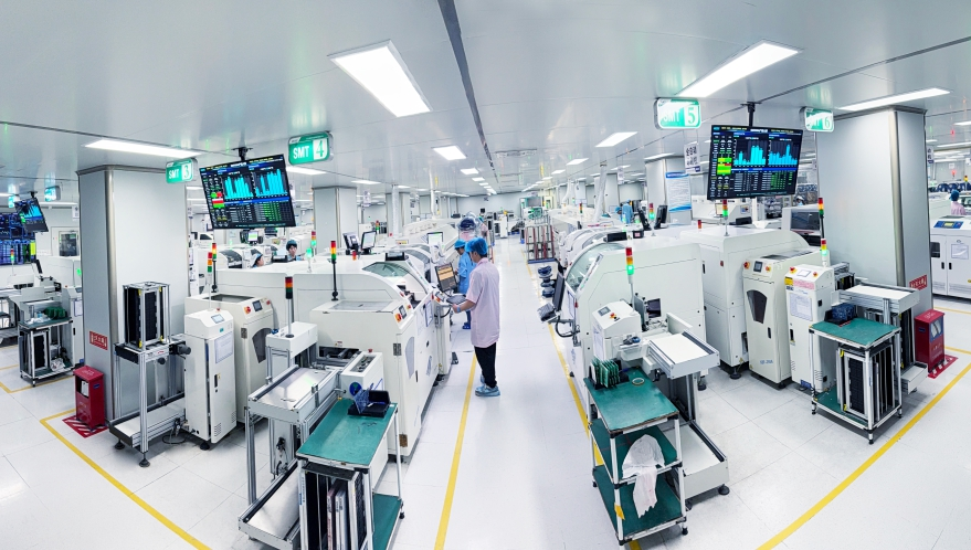
SMT Sector

SMT Sample

SMT Sample

DIP Sector

DIP Sector

Component Warehouse

Component Warehouse

Samples Warehouse for Shipment
Need Technical Details?
Contact us for detailed specifications and capability discussions.
Technical Enquiries
Talk to Our Engineers
Contact Us →